CNC Machining for Semiconductor Equipment: Cleanliness, Materials and Tolerance
What semiconductor equipment makers actually require from a machining partner: geometry-class tolerances, particle and residue control, material certification, and why one-setup machining decides the geometry callouts.
Semiconductor equipment is the hardest mainstream customer in machining, and most of the difficulty never shows up in a single dimension on the drawing. Since 2025 we have delivered core precision parts to the world's leading lithography equipment maker, and those programs reshaped how we plan every semiconductor job. Here is what the sector actually demands.
Geometry Stacks Beat Single Dimensions
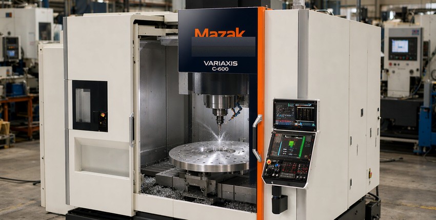
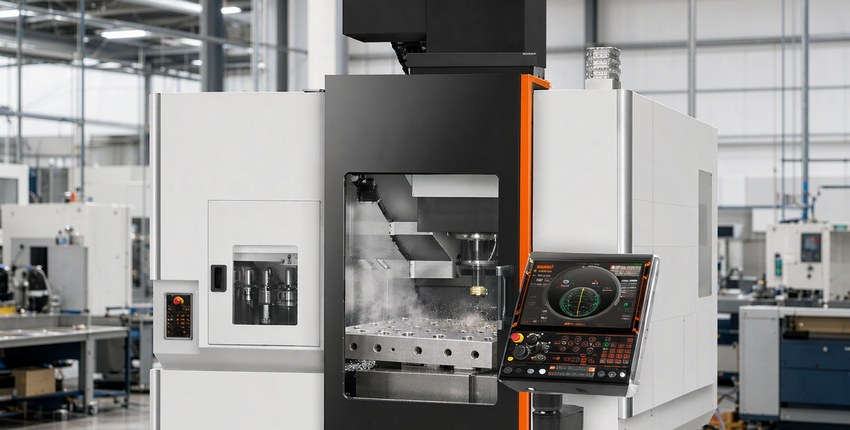
A fixture plate can have every size within tolerance and still fail, because the callouts that matter are geometric: flatness across 400 mm, parallelism between bores, coaxiality between feature systems. These stack with every setup the part sees. The practical answer is five-axis machining in one clamping for feature-dense parts, which is why 11 Mazak five-axis centers anchor our fleet. Fewer setups, fewer stacked errors, fewer surprises at your incoming inspection.
Thin Walls and Stress
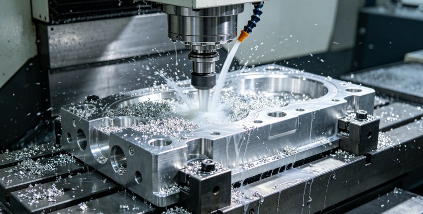
Chamber components and sensor mounts often specify walls near 0.3 mm. At that scale the material's internal stress, not the cutting force, is the main enemy. Our five-step sequence (rough, natural aging, semi-finish, stress release, finish) exists for exactly these parts. Skip the aging steps and the wall measures true on the CMM and false in your vacuum chamber a week later.
Materials: Stainless, Aluminum, and the In-Betweens
Work-hardening 304, anodized 6061, and specialty alloys dominate semiconductor hardware. Each brings a control problem: 304 wants constant tool engagement to avoid hardening; anodized parts need masking discipline before finishing; every alloy needs mill certificates traceable to heat numbers because contamination outgasses in vacuum. Our stainless selection guide covers the 304 machining behavior in detail.
Cleanliness Is a Specification
Parts for vacuum and wafer-adjacent service get cleaned, dried, and packed in a controlled sequence. Oils, fingerprints, and cutting residue that a machine shop ignores become particle sources in your chamber. We treat cleaning and packaging as process steps with written instructions, not as shipping chores.
Documentation the Programs Expect
- Full dimensional reports tied to drawing balloons.
- Material certificates with heat numbers.
- Process change control: no routing change without written approval.
- On-time delivery measured against program schedules, not monthly averages.
That last point matters more than any tolerance. Equipment makers plan module builds months ahead, and a part that arrives late by two weeks costs more than a scrapped batch.
How to Qualify a Shop for This Work
Ask three questions. Can you hold geometry-class tolerances, and how do you measure them? What is your stress-relief sequence for thin walls? Who signs off process changes? The answers separate semiconductor-grade shops from general precision shops. Our semiconductor industry page and the thin-wall case study show the work itself.
Related Articles
More from the Semiconductor series.
Have a project in mind?
Send drawings to kgl@kglmfc.com or request a quote. We respond within 24 hours.
Request a Quote