CNC Machining for Semiconductor Equipment: Materials and Key Components
Materials and machined components for semiconductor equipment: vacuum chambers, wafer handling parts, gas distribution, and the aluminum, stainless, titanium, and PEEK choices and finishes behind them.
Semiconductor equipment is unforgiving in a specific way: the parts do not carry dramatic loads, they just have to stay clean, stable, and dimensionally honest through millions of cycles in vacuum, plasma, and process chemistry. We machine components for semiconductor and related high tech equipment, and our semiconductor machining page shows the part families. Two of our earlier posts cover tolerances and CMM verification and the equipment side in depth; this one is the materials and components map we use when a new drawing arrives.
1. What the environment demands
Three requirements shape every decision. Vacuum integrity: chambers and flanges must seal reliably, which pushes surface finish and flatness callouts tighter than the loads alone would justify. Particle control: anything that sheds, burrs, or traps residue inside a chamber becomes a defect on a wafer, so deburring, edge finishing, and cleaning are part of the route, not extras. Stability: parts see temperature swings and reactive gases, so the material and its finish must stay inert and dimensionally calm in service, not just on the inspection bench.
2. The materials, and what each one is for
Aluminum dominates the structural side. 6061, 6063, and 7075 go into chambers, base plates, chuck bodies, and gas distribution components because they machine cleanly, conduct heat, and take anodizing well. Our aluminum guide covers the alloys, and the anodizing choices are explained in our anodizing types guide.
Stainless steel takes the strength and vacuum hardware roles: 304 and 316L for fittings, flanges, fasteners, and process gas components, usually passivated or electropolished so surfaces stay inert and particle free. Grade selection and the welding question are covered in our 304 vs 316 comparison.
Titanium appears where strength to weight and corrosion resistance both matter, in structural and motion components. Engineering plastics close the list: PEEK and PTFE insulators, probes, and sealing components, where electrical isolation and chemical resistance are the point. Our PEEK page covers the machining side.
| Material | Key properties | Typical applications | Common finishes |
|---|---|---|---|
| Aluminum 6061 / 6063 / 7075 | Lightweight, thermal conductivity, machinable | Chambers, base plates, chucks, gas distribution | Anodizing, natural or hard |
| Stainless steel 304 / 316L | Corrosion resistant, vacuum compatible | Fittings, flanges, fasteners, gas components | Passivation, electropolishing |
| Titanium Ti-6Al-4V | High strength to weight, corrosion resistant | Structural parts, motion components | Bead blasting, anodizing |
| PEEK / PTFE | Electrical insulation, chemical resistance | Insulators, probes, sealing components | As machined, cleaned |
3. The components we see most
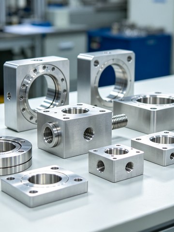
Vacuum chambers and flanges lead the list. Bolt patterns, sealing faces, and port geometry all carry real tolerance, and the sealing face finish decides whether the seal holds over millions of cycles. Wafer handling components, end effectors, chucks, and load ports, add scratch free surfaces and complex geometry on top of tight tolerance. Gas distribution parts, showerheads, distribution plates, and RF shielding, are decided by hole geometry: thousands of small features whose consistency at scale is what the process actually feels. Frames and cooling components close the list with large envelopes and flatness controlled mounting faces.
4. Where the difficulty sits, and what we change
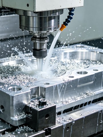
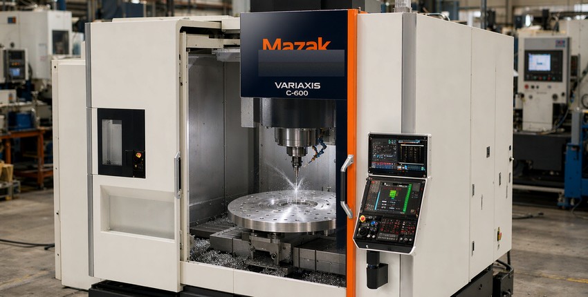
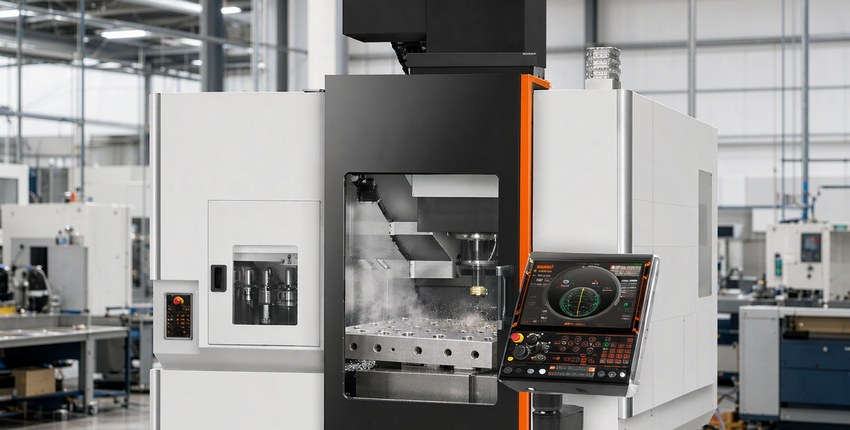
Large parts fight thermal growth and fixturing deflection, so rigid fixturing, controlled environments, and in process measurement carry the tolerance; complex contoured features go to five axis work to cut setups and stacking error, described on our five axis page. Burrs and machining residue are unacceptable inside a chamber, so deburring and cleaning are scheduled operations with inspection after them, not a packing step. And because our standard tolerance on machined features is plus or minus 0.005 mm, with tighter bands on specific features under full CMM verification, the drawing tells us where the process needs to concentrate instead of guessing.
5. Traceability, because the audit arrives eventually
Semiconductor customers expect the paper to match the parts. Material certificates travel with every order, first article and lot inspection reports are produced under our ISO 9001:2015 system, and our ISO 13485:2016 and AS9100D scopes cover the customers whose documentation requirements go further. Records are kept per order, so when an auditor asks how a chamber was made and verified three years ago, the answer exists.
6. FAQ
Which finish for aluminum vacuum components?
Usually anodizing, Type II for general protection and Type III where wear or hardness matters. The coating is planned into the dimension chain so sealing faces land on target after finishing.
Can you hold tight tolerance on large chambers?
Yes, with process design: rigid fixturing, controlled cutting sequence, in process measurement, and CMM verification of the critical features. Large is a cost question, not a capability question.
Do you supply PEEK insulators and sealing parts?
Yes. PEEK and PTFE insulators, probes, and seals are regular work; stress relief and sharp tooling keep the geometry stable. See our PEEK machining page for the process details.
What documentation ships with an order?
Material certificates, first article and lot inspection reports, and process records kept per order under ISO 9001:2015. Additional documentation under our ISO 13485 and AS9100D scopes where the customer requires it.
If you are sourcing machined components for semiconductor equipment, send your STEP or IGES models and 2D drawings to kgl@kglmfc.com or request a quote on our RFQ page. We will review the materials, finishes, and tolerance callouts, and return a quote within 24 hours.
Related Articles
More from the Semiconductor series.
Have a project in mind?
Send drawings to kgl@kglmfc.com or request a quote. We respond within 24 hours.
Request a Quote