CNC Machining for Semiconductor Equipment
Ultra-precision components for semiconductor equipment makers. Vacuum chamber flanges, optical encoder mounts, polarization controllers, lens barrels, and thin-wall stainless steel parts.
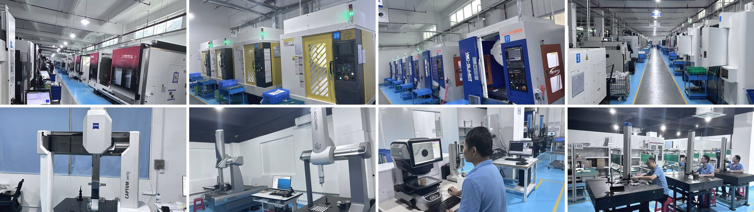
Inside the KGL shop floor · tour our 6,000+ m² facility
Semiconductor Equipment Parts
KGL machines ultra-precision components for semiconductor equipment manufacturers. Our 5-axis Mazak centers and Hexagon CMM (0.0015 mm accuracy) deliver the geometric precision and surface finish that semiconductor applications require.
Typical Parts
- Chamber components and shielding
- Electrode and focus ring components
- Precision mounting plates
- ESD-sensitive components in conductive plastics
Materials
Aluminum (6061-T6, 7075), stainless steel (316L, 17-4PH), PEEK, PEEK1000, PEI, ESD225, ESD420, and conductive nylon.
Cleanliness and Packing
Chamber components, fixtures and vacuum-adjacent parts are deburred, ultrasonically cleaned, dried and sealed in PE bags; nitrile-glove handling and cleaning records ship with the inspection report. Thin-wall geometries are CMM-verified on Hexagon and Zeiss machines before release, so flatness and coaxiality arrive as documented values, not promises.
Typical parts: 10 part families with tolerances and typical order sizes.
Process Coverage for Semiconductor Programs
Semiconductor equipment parts combine tight geometry with cleanliness requirements. We machine them on 11 five-axis Mazak centers for optical and vacuum geometries, with turning cells for lens barrels and sealing joints, and a dedicated support cell for wire EDM features. Chamber-adjacent parts are deburred, ultrasonically cleaned, dried, and sealed in PE bags, with nitrile-glove handling and cleaning records shipped alongside the inspection report.
Tolerances, Materials and Documents
| Feature class | Standard capability | Verified by |
|---|---|---|
| Alignment and mounting interfaces | ±0.005 mm | CMM report per lot |
| Thin-wall flatness and coaxiality | within 0.01 mm | Hexagon / Zeiss CMM |
| Optical seating faces | Ra 0.4 or better | Surface roughness records |
| ESD-grade plastics machining | ESD225 / ESD420, conductive nylon | Material certificates |
Materials in regular production include 6061-T6 and 7075 aluminum, 316L and 17-4PH stainless steel, titanium, PEEK, PEI, and ESD-grade plastics. Documentation packages cover material certificates, FAI, and batch dimensional reports for your equipment qualification files.
Semiconductor Equipment Parts in Production
8 documented part families. Every part below opens its own detail page with photos, material notes, and tolerance data.
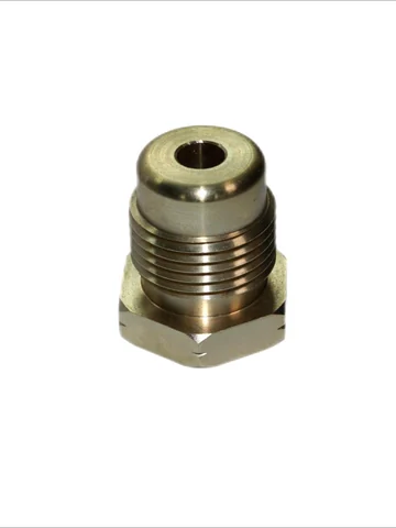
Semiconductor Equipment
Titanium Alloy Lens Gasket Sealing Joints
View product →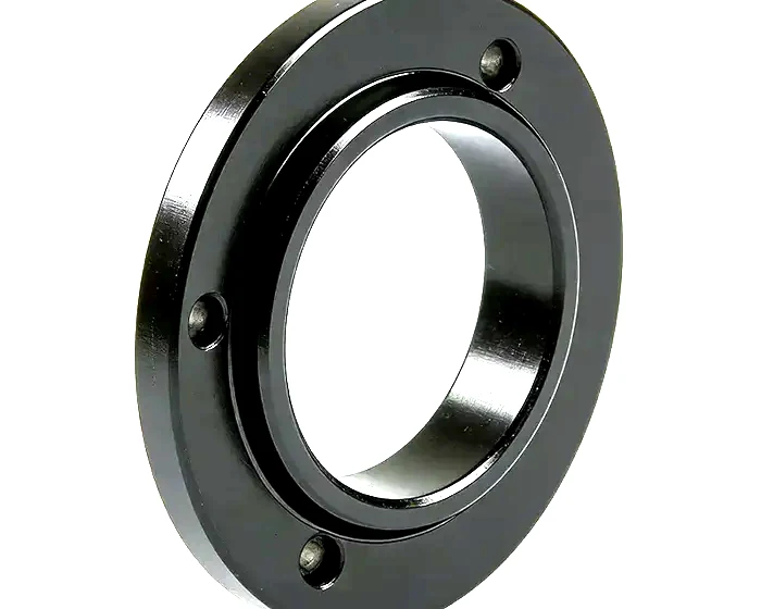
Semiconductor Equipment
Polarization Rotation Controller
View product →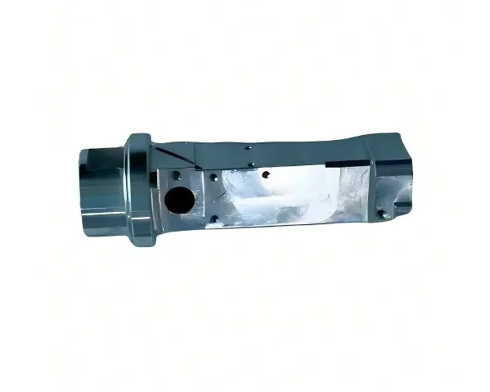
Semiconductor Equipment
High-Precision Optical Housing (Lens Barrel Holder)
View product →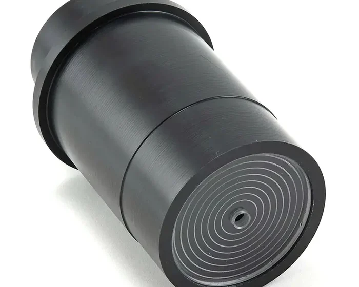
Semiconductor Equipment
Laser Collimator Adjustment Seat
View product →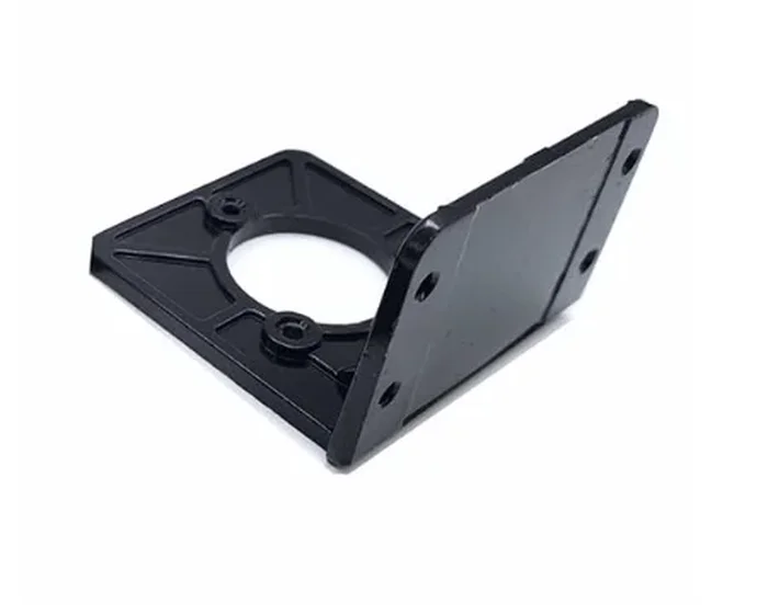
Semiconductor Equipment
Optical Encoder Mounting Bracket
View product →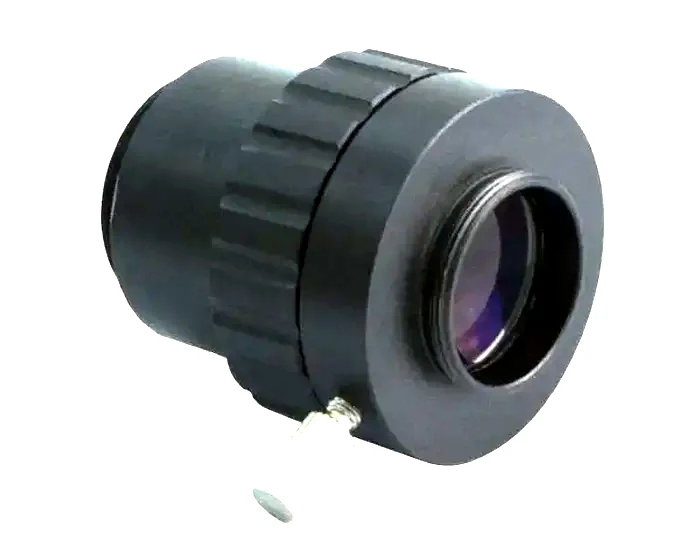
Semiconductor Equipment
Optical Microscope Adjuster
View product →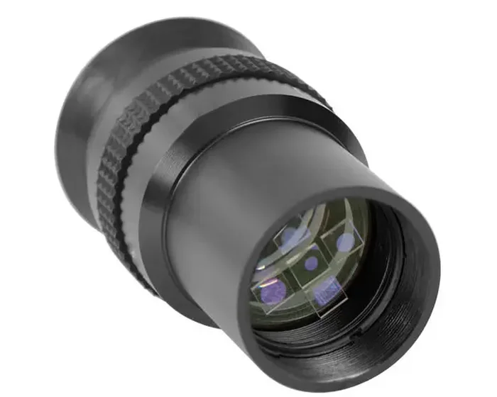
Semiconductor Equipment
Optical Rotating Eyepiece
View product →
Semiconductor Equipment
High-Precision Connector Body for Optoelectronic Communication
View product →Questions buyers ask before the first order
How thin can you machine stainless steel walls?
For the world's leading lithography equipment maker we delivered SUS304 parts with 0.3 mm walls in a 150 x 45 x 6 mm envelope, with flatness, position and coaxiality within 0.01 mm.
What is your measurement accuracy?
Hexagon CMMs with 0.0015 mm accuracy verify every critical dimension, backed by 40+ precision inspection instruments.
Do you machine ESD-safe plastics?
Yes. ESD225, ESD420, conductive nylon, PEEK and PEI for ESD-sensitive components.
Can you reach Ra 0.4 surface finish?
Yes. The referenced SUS304 parts were delivered at Ra 0.4 um. Grinding and finishing are sequenced in house, so the datum chain is never broken.
Do you sign NDAs before reviewing drawings?
Yes. A standard mutual NDA is available before any drawing or specification is shared.
What is the lead time for semiconductor equipment parts?
Quotes in 24 hours; prototypes typically 7 to 15 days, longer for multi-process routes that add grinding or EDM.
Engineering reference behind this page
The tables and bands the sections above rest on, kept by the same engineering team that runs the work.
- Sealing facesRa and Rz that decide leak rate on a vacuum side part.
- Flatness and parallelismHow the flatness callout is stated and how it is verified.
- Flatness by processWhich operation reaches the flatness a seal actually needs.
Full index, including material grades and surface finish data: engineering reference hub.
Have a Project in This Industry?
Send your drawings and get a quote within 24 hours.
Request a Quote