CNC Parts for Semiconductor Equipment: What Cleanroom-Ready Machining Means
What cleanroom-ready means for machined semiconductor parts, which aluminum, stainless and engineering plastics hold up inside tools, how burr control and cleaning are sequenced, and what tolerances and documentation buyers should demand.
Cleanroom-ready CNC machining means the finished part will not contaminate the controlled environment it enters. In practice that covers four things: edges and surfaces that do not shed particles, materials that resist outgassing, plastics that manage static charge, and cleaning plus packaging that keep the part clean until installation. It also means the dimensions were verified rather than assumed. This article explains what semiconductor equipment buyers should check, how machining for cleanroom parts differs from general CNC work, and how we handle it on our floor, where 100+ CNC machines, including 11 five-axis centers, have cut aluminum, stainless steel and engineering plastics for equipment builders since 2013.
1. What does cleanroom-ready actually mean for a machined part?
A cleanroom is graded by how few particles its air carries. Equipment builders assemble wafer handling, metrology and optics inside those rooms, and every component they bring in either respects that air or ruins it. A machined part becomes a contamination source in four ways: sharp edges and burrs that shed metal particles when handled, chips packed into blind holes, coolant or cutting-oil residue that slowly outgasses, and plastics that generate static and attract dust. Cleanroom-ready machining closes each path before the part ships.
That work has little to do with the machine brand and everything to do with discipline. Edges get a consistent 0.1 to 0.3 mm break instead of random hand deburring. Blind holes are drilled with chip escape in mind. Plastic parts are machined with sharp tools so surfaces seal rather than fuzz. One honesty note: our machining happens in a normal workshop, not inside a cleanroom. Cleanroom-ready describes the condition of the part when it arrives at your receiving bench.
2. Which materials hold up inside semiconductor equipment?
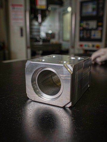
Aluminum carries most of the structural load in semiconductor tools. We machine 6061 and 7075 for frames, brackets and manifolds, and MIC-6 cast plate when a fixture needs flatness without stress movement. Hard anodizing adds surface hardness and keeps oxide from rubbing off into the air stream. For gas delivery and chamber hardware, 316 stainless resists corrosion, and 17-4PH brings strength where threads and thin walls see load.
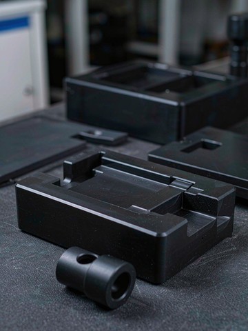
Plastics do the jobs metals cannot. PEEK and PEI machine clean, resist heat and release very few particles, which is why they appear in wafer handling and insulating positions (our PEEK and engineering plastics guide covers the grades). Where static threatens devices, we machine ESD-safe grades such as ESD225 and ESD420 into test fixtures and carriers; the black parts in the photo below are from that family. Ceramics like zirconia and alumina cover the extreme insulation positions. The full range is listed on our materials page.
3. How does the machining process change for these parts?
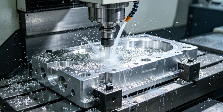
Burr control leads the list. We program the edge break into the toolpath with the same tool that finishes the surface, so edge quality does not depend on who deburrs the part by hand. Where hand work is unavoidable, it happens under magnification against a written spec. Coolant strategy matters too: high-pressure flushing clears chips from deep pockets, because a chip left behind is a particle waiting to escape.
Cleaning is its own process step, not an afterthought. Parts are washed ultrasonically, rinsed in deionized water, dried immediately, and sealed in bags before they touch an open bench. Handling moves to nitrile gloves and ESD-safe containers. None of this is exotic; it is sequencing, and it is written into the job traveler so it repeats on order number fifty as well as order number one.
4. What tolerances and surface finishes do these parts need?
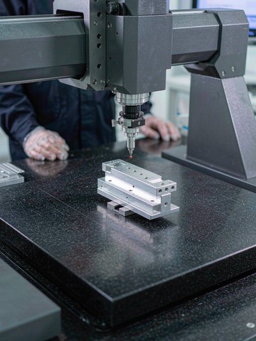
Standard tolerance on machined features is ±0.005 mm, and most semiconductor hardware lives comfortably inside that band. Where a drawing asks for more, ±0.002 mm is possible only for specific features on five-axis work, and only when the part is verified with full CMM inspection; our Hexagon and Zeiss machines hold 0.0015 mm accuracy. Flatness on seal faces and vacuum interfaces usually decides success more than hole positions do.
Surface finish follows the function. Sealing surfaces run Ra 0.4 to 0.8 um; anodized fixture plates trade a little finish for wear life. Coatings need planning: anodizing grows thickness outward, so threaded holes and bearing bores are masked or the dimensions shift. We put those decisions on the quote, not in a footnote, and our surface treatment page shows the standard options.
5. How do we verify and document a cleanroom-ready part?
Verification is where cleanroom-ready claims get tested. With 40+ inspection instruments, including CMMs, vision systems and roughness testers, every dimensioned feature on the drawing lands on the inspection report, and first article inspections follow the same CMM workflow we use for aerospace work. Material certificates travel with the shipment under our ISO 9001:2015 system, and our AS9100D and ISO 13485:2016 registrations keep the documentation habits sharp across industries. Components we machine for the world's leading semiconductor lithography equipment maker have raised our own bar on what documented means.
Packaging closes the loop: sealed bags, part-specific protection, and reports in the box. We hold 177 customer records in our CRM, 84 of them overseas across 19+ countries, and the same 24-hour quote process applies: send complete 2D and 3D files through our RFQ page and a machinist, not a salesperson, reviews them the same day. No minimum order applies to prototypes. Buyers comparing suppliers across the industry can start from our semiconductor machining page.
From Our Shop Floor: Cleaning an ALD Chamber Block
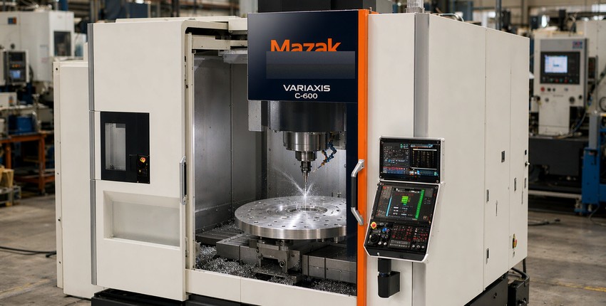
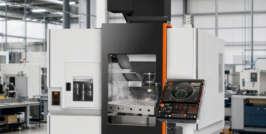
A vacuum chamber block for an ALD tool shows how far the cleaning discipline has to go. The part is 6061-T6, machined on a Mazak VARIAXIS C-600 five-axis center. Programmed R0.5 chamfers break the edges inside the toolpath, and the roots of cross holes get hand-scraped with a ceramic scraper because no end mill reaches that corner cleanly. Cleaning runs in a fixed sequence: 40 kHz ultrasonic wash for 10 minutes in a semiconductor-grade neutral detergent, two deionized water rinses, then a 30 minute bake at 110°C. Packing runs three layers: vacuum bag, desiccant and an ESD bag. That sequence exists because a customer once reported 0.05 mm aluminum chips left on a chamber face. We added a white-glove wipe and a magnifier check at final inspection, and the defect rate on that part family went from 1,200 PPM to zero.
Frequently Asked Questions
What does cleanroom-ready mean for a machined part?
It describes a part prepared to enter a controlled environment without contaminating it: burr-free edges, low-outgassing materials, ESD-safe plastics where static matters, verified dimensions, and sealed packaging. The machining happens in a normal workshop; the discipline shows up in the finishing, cleaning and documentation.
Which plastics are suitable for semiconductor fixtures?
PEEK, PEI and PI for low particle release and heat resistance, plus ESD-safe grades such as ESD225 and ESD420 where static discharge threatens devices. Grade choice depends on temperature, stiffness and whether the fixture touches wafers directly.
What tolerance can you hold on semiconductor equipment parts?
±0.005 mm as standard on machined features. ±0.002 mm is available only for specific features on five-axis work and only with full CMM verification on machines holding 0.0015 mm accuracy.
Do you provide inspection reports and material certificates?
Yes. Every dimensioned feature appears on the inspection report, first articles follow our CMM workflow, and material certificates ship with the parts under our ISO 9001:2015 system.
How fast can you get a quote?
Quotes come back within 24 hours for complete 2D and 3D files, with no minimum order for prototype parts.
This article is general engineering guidance, not a binding manufacturing guarantee. Tolerances are confirmed per part based on geometry, material and inspection requirements. Request a formal quotation for part-specific specifications.
Related Articles
More from the Semiconductor series.
Have a project in mind?
Send drawings to kgl@kglmfc.com or request a quote. We respond within 24 hours.
Request a Quote